Project Category: Electrical
Join our presentation anytime between 10AM and 12:30PM on Tuesday April 5th
About our project
The primary component of any camera is the image sensor. These sensors are used in mobile phones, cars, security systems, and other such devices. Complementary Metal Oxide Semiconductor (CMOS) and Charge-Coupled Device (CCD) image sensors are the two technologies currently dominating the market. The biggest advantages that CMOS image sensors have over CCD image sensors is the fundamental similarity with other digital systems. This allows the sensor and the Digital Signal Processing(DSP) units to be fabricated on the same chip. To do this, an Analog-to-Digital Converter (ADC) must convert the analog pixel voltage to its equivalent digital representation. The use of on-chip ADCs allow for noise reduction, faster conversion times, and improved system integration. This means a higher frame rate, improved image quality, and a more configurable interface between the image sensor and external digital systems.
The I2Sense Lab at the University of Calgary specializes in CMOS image sensor research. However, they have not used internal ADCs in their previously fabricated image sensors. Our team successfully designed and will fabricate a compact 12-bit ADC to realize high-resolution and high-speed digital cameras.
Meet our team members
Riley Bahl:
Riley is a 4th year electrical engineering student. His technical interests include FPGA, SoC, and ASIC design. He has 3 years of experience in digital design, digital logic, and signal/image processing with Verilog/VHDL and embedded-C. He is interested in innovative entrepreneurship and wants to develop new technologies for industrial applications.
Robert Dewar:
Robert is a 4th year electrical engineering student with a minor in computer engineering. His technical interests include analog IC and firmware design. He has experience with FPGA design in Quartus, Arduino design, and programming in Python, Java, C and MATLAB.
Maaz Khurram:
Maaz is a final-year electrical engineering student with a minor in Computer Engineering. His technical interests are in PCB design and analog design. He has previous internship experience in designing robust low-power 2.4GHz consumer electronics at Garmin. He loves tinkering and talking circuits.
Polukh Polukhov:
Polukh is a 4th year electrical engineering student following the general degree stream, with interests in embedded systems, analog IC design, and mechatronics. His previous experience includes FPGA design using Quartus, PCB design using Altium, and working with STM32 microprocessors for on-board computers.
Leo Rogers:
Leo is a 4th year electrical engineering student with interest in the design and control of dynamic systems. He has experience creating PID controllers in Python and MATLAB. He is also interested in digital circuit design with some previous experience in FPGA development using Quartus.
Wayne Weaver:
Wayne is a 4th year electrical engineering student with a previously completed Computer Engineering Technology diploma. His technical interests include tinkering to gain understanding and creative troubleshooting. He has previous experience with FPGA development with Quartus, control systems in Simulink / MATLAB and various programming languages.


Details about our design
HOW OUR DESIGN ADDRESSES PRACTICAL ISSUES
Camera technology has significantly improved over the course of the last 30 years. Two of the current contributors in this technology are the Complementary Metal Oxide Semiconductor (CMOS) and Charge-Coupled Device (CCD) image sensors. The benefits of a CMOS system is that the entire camera can be manufactured on a single chip. This means that only a single fabrication run is needed, resulting in a smaller system and cheaper means of production. Additionally, CCDs continue to be used due to producing a slightly better image quality. However, as technology continues to improve the difference in the image quality decreases. In order to maximize the benefit of a CMOS image sensor’s lower footprint Analog to Digital Converter (ADC) designs need to be constructed and realized.
WHAT MAKES OUR DESIGN INNOVATIVE
For the I2Sense lab, this will be the first chip fabricated with an integrated ADC contained within the same chip as the image sensor.
WHAT MAKES OUR DESIGN SOLUTION EFFECTIVE
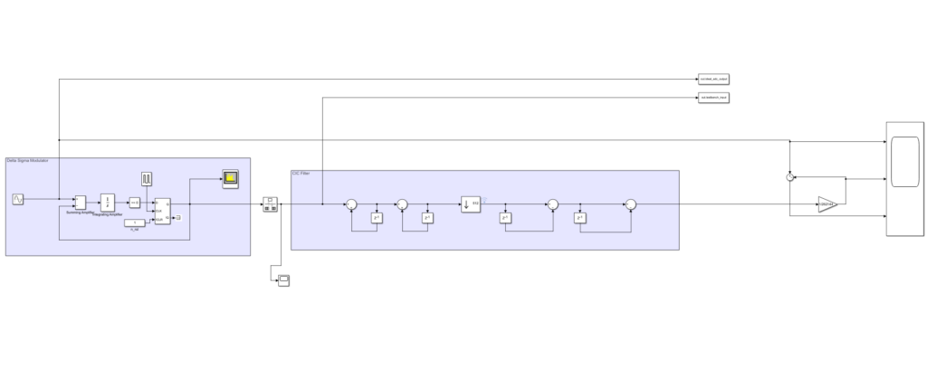
During the process of determining the best architecture to use to meet the constraints provided for the project, the team came to the conclusion that the biggest consideration would be the amount of area used by the ADC. A Delta Sigma ADC was the best solution to meet the space and resolution requirements of the project. A brief overview of the system, what it does and how it operates, can be summarized as:
- The Delta Sigma ADC takes in an analog voltage produced by the image sensor’s pixel and converts it to a Pulse Code Modulated (PCM) signal with the maximum sample rate of 1MS/s. For higher magnitude inputs, the pulse is 1 for more of the period and for lower magnitude signals, the pulse is 0 for more of the period.
- The PCM signal is then sent to the Cascaded Integrated Comb (CIC) filter which down samples and averages the PCM by a factor of 512, producing one averaged output per 512 samples of the PCM signal, outputting it as a 12-bit number.
- This 12-bit number is a digital representation of the voltage on the pixel. The stored voltages can then be used to recreate the image from the sensor, since the voltage on the pixel is related to the wavelength and intensity of light incident on the pixel.
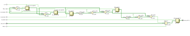
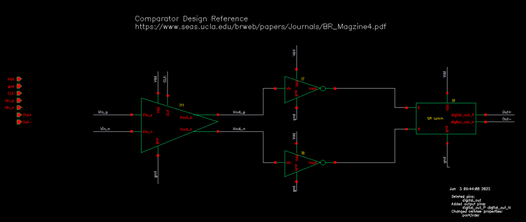
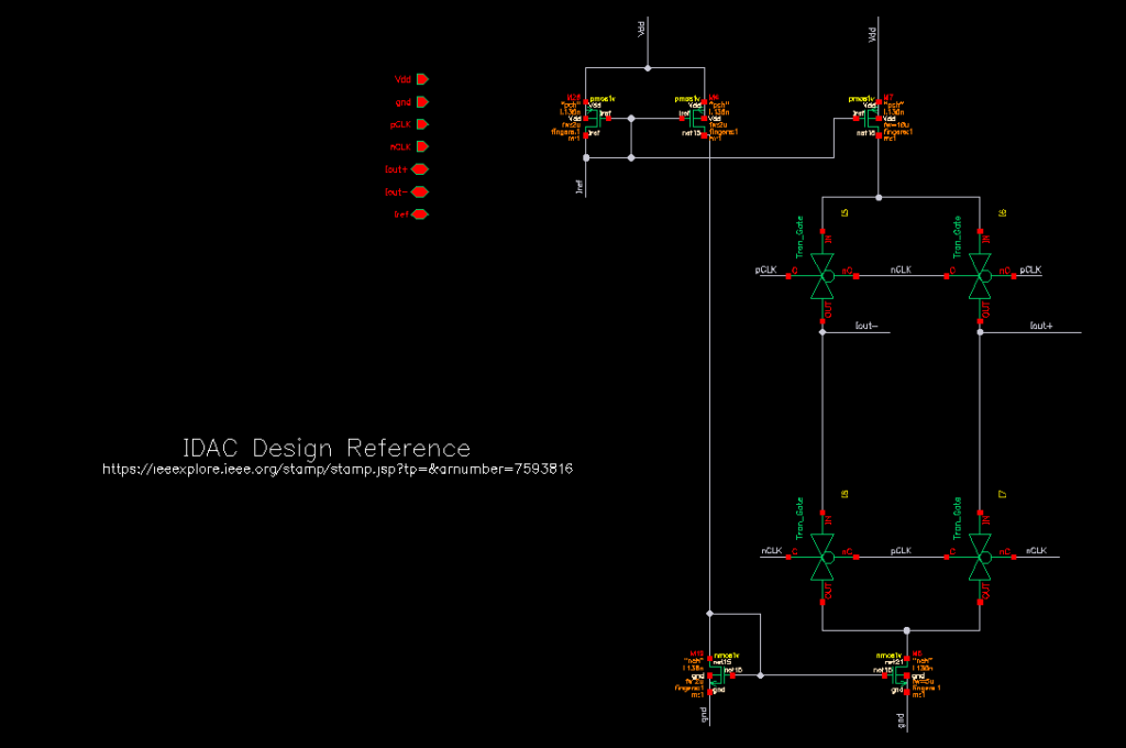
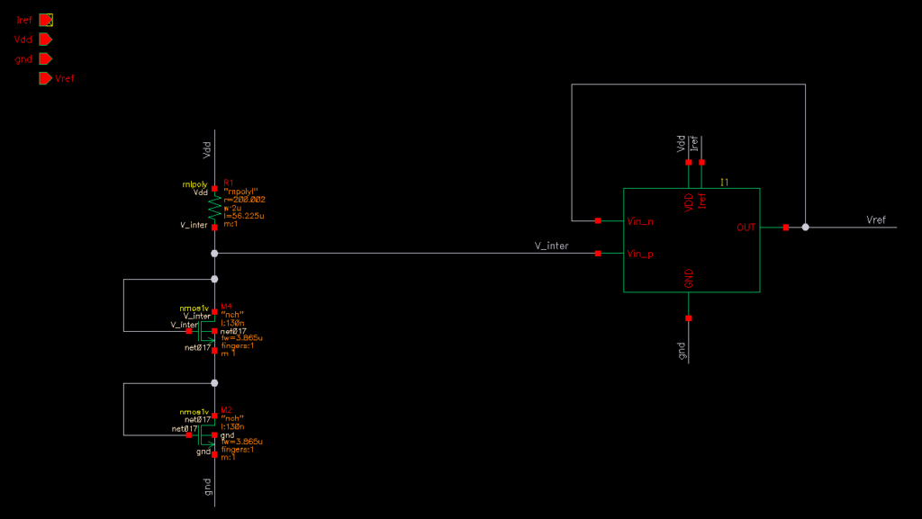
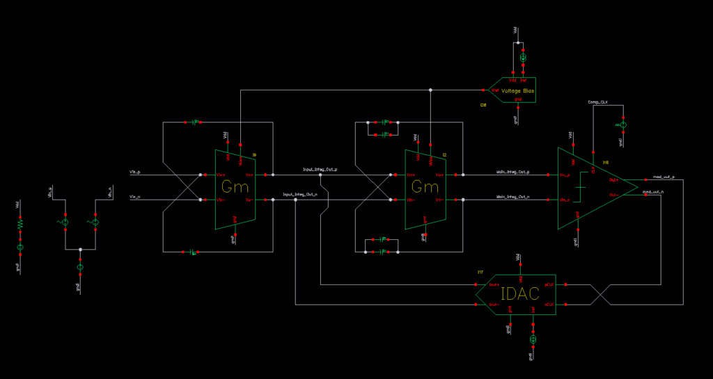
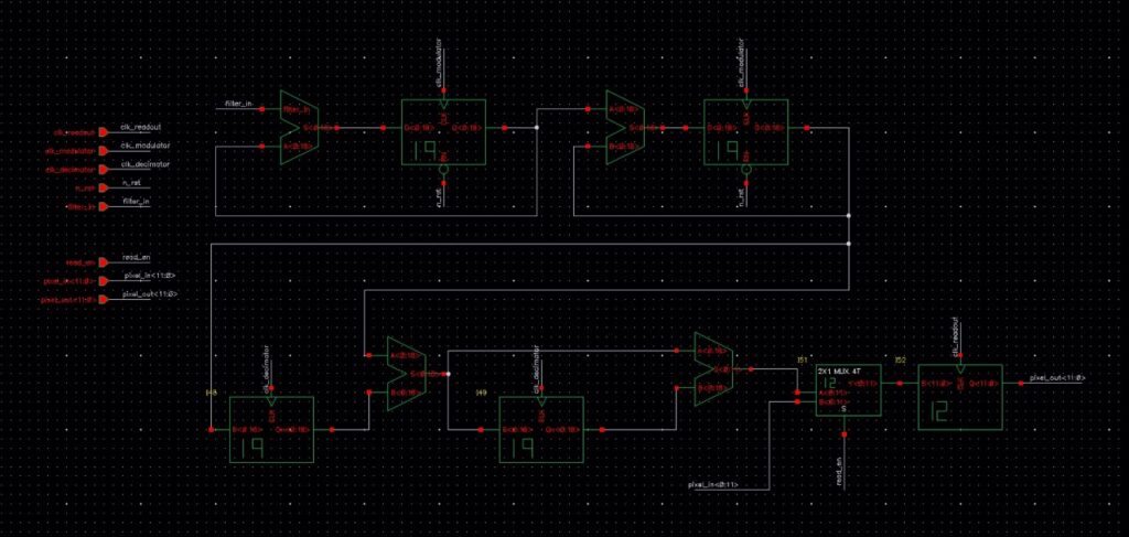
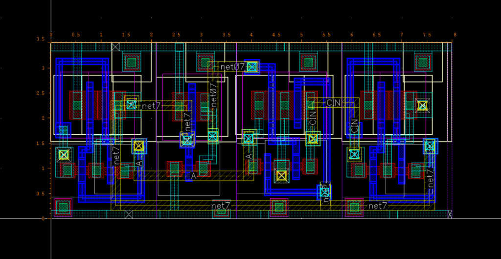
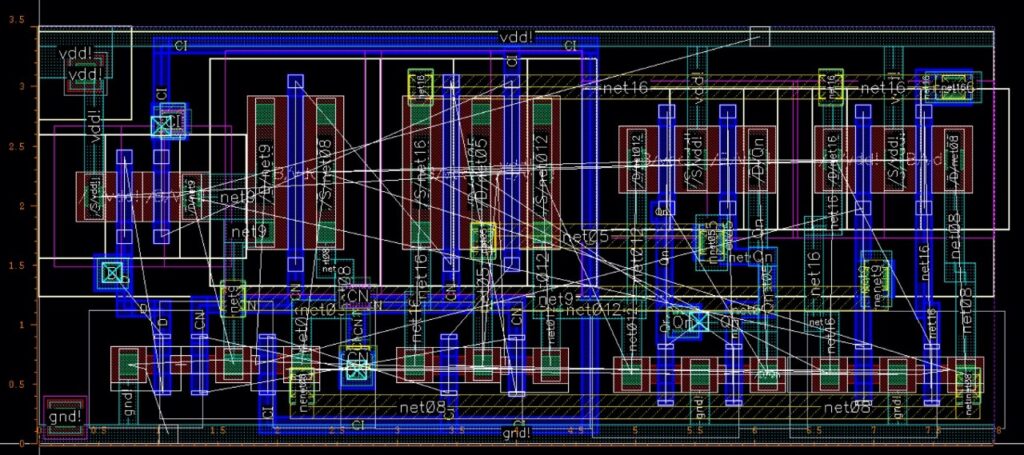
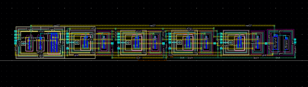
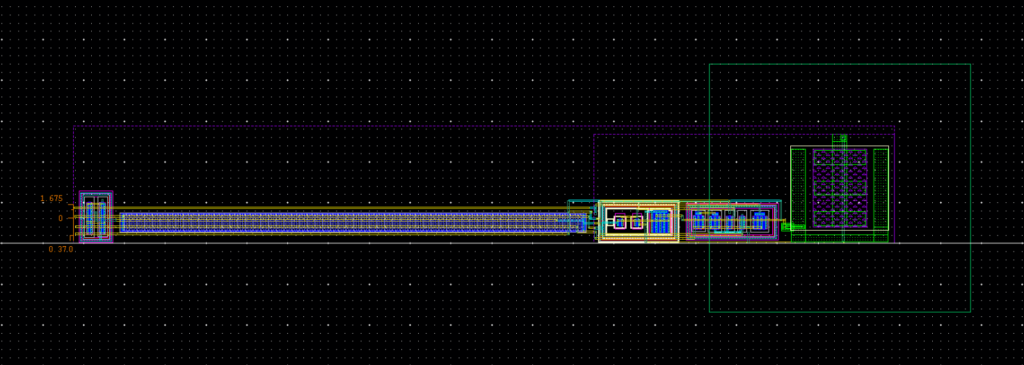
The design solution is developed in stages, with an initial logical description of the system being created in Simulink (Figure 1). From there, the analog side begins development in Virtuoso and the digital side using the Matlab Filter Designer tool to generate Register Transfer Level (RTL) code for the digital CIC filter. Vivado is then used to adjust the auto generated RTL code (Figure 2). At this stage the plan was to have the team break into different design methodologies for analog and digital. With the analog team continuing to develop the Delta Sigma ADC in Virtuoso and the digital team using the automated place and route of RTL code available for digital logic through Genus and Innovus. Due to complications, the digital library for the technology node was not received. Therefore, the digital team shifted to using the analog design flow in Virtuoso. From there, schematic descriptions of the design were created for the various components of the ADC and filter, the digital components are consistent with well documented designs of digital logic elements so the schematic views of digital subcomponents will not be posted (Figures 3 to 6). This was followed by schematics for the complete analog and digital sections (Figure 7 and 8). Finally, the positive output of the comparator is connected to the filter in of the digital filter. Multiple sets of iterations were done until performance specifications were met, allowing work to begin on layout. Shown in the photo gallery are some examples of subcomponent layout, the entire system layout is not human readable due to scale (Figure 9 and on). The team focused on starting with the subcomponents of each section and tiling the design together. Tiling the ADC with the filter was the last step. Once the layout is completed the design files will be sent for fabrication.
HOW WE VALIDATED OUR DESIGN SOLUTION
The verification of the design solution, like the design itself, was completed in stages:
- The initial verification was completed using the logical model developed in Simulink. This gave the team an idealized view of the systems performance and a baseline to compare the actualized design to.
- The next stage initially differed for the analog and digital teams. After the logical performance was verified, the analog team began making subcomponent schematics in Virtuoso and simulating them with the Analog Design Environment (ADE). This gave non idealized views of the system behavior modeling the signal rise times, steady state errors, and a number of other performance issues not seen in the idealized logical view.
- The digital team at this stage used Vivado to generate a testbench and output the data generated by the RTL code to MATLAB to have its performance measured. This, however, didn’t account for physical effects of actual components, but allowed for better understanding of required clock timing and signal propagation requirements. The digital team would then have used automated tools to perform place and route after providing performance, power, and area constraints. After place and route, simulations would have been run on the various stages of the design using tools like Xcelium. Since the digital library wasn’t received, the verification was completed using the same process as the analog team.
- Schematic views of components were created for both the analog and digital sides and tested. Different configurations for the subcomponents were tested to find which best met the constraints with as little trade off as possible. As new constraints were discovered over the course of the design process, adjustments were made throughout the entire process.
- Subcomponents were connected and tested with other components in isolation of the rest of the system. These were then adjusted if unforeseen issues were present, and slowly the system began to come together as each level was verified.
- Due to time constraints, layout began before the full chip schematic simulations had been verified. Design Rule Check (DRC) was used to ensure manufacturability of layout and Layout Versus Schematic (LVS) was used to ensure the layout connections matched the schematic. Finally, post layout simulations were run to ensure added parasitic effects of layout didn’t drastically impact system performance.
- Complete schematic ADC simulations were run and verified in isolation of the filter. Complete filter schematic simulations were run and verified in isolation of the ADC.
- Complete system schematic simulations were run to verify performance when everything was connected.
- Layout of full filter and full ADC was completed and verified with DRC and LVS separately, and post layout simulations were conducted.
- After the final layout of the entire system was completed, tests were run, and performance was verified.
FEASIBILITY OF OUR DESIGN SOLUTION
The process of designing integrated circuits follows the design process outlined in What Makes Our Design Solution Effective, and once the design files are generated, they will be sent to a facility capable of manufacturing Integrated Circuit (IC) chips to be produced.
Partners and mentors
The team would like to thank the capstone sponsor, Devin Atkin and the I2Sense laboratory for the valuable support and guidance throughout the year. Additionally, the team is grateful for the access and introductory lessons for the cadence design tools for designing the ADC. The team would also like to thank our academic advisor Mohamed Balla Elamien Mohamed and our TA Zahra Kabirkhoo for the assistance and feedback they provided throughout the project. Finally, we would like to thank Dr. Yadid-Pecht for providing in-depth image sensor understanding through the Imagers and Integrated Micro-Nano Sensory Systems course.
Our photo gallery

References
[1] B. Razavi, Design of analog CMOS integrated circuits. New York: McGraw Hill Education, 2017.
[2] E. Smith, “Understanding the delta-sigma ADC – Technical Articles,” All About Circuits. [Online]. Available: https://www.allaboutcircuits.com/technical-articles/understanding-the-delta-sigma-analog-to-digital-converter/. [Accessed: 30-Oct-2021].
[3] T. C. Carusone and D. A. Johns, Analog Integrated Circuit Design. Wiley.
[4] B. Razavi, “The strongarm latch.” [Online]. Available: https://www.seas.ucla.edu/brweb/papers/Journals/BR_Magzine4.pdf. [Accessed: 30-Oct-2021].
[5] Lo, Tien-Yu, and Chung-Chih Hung. “Chapter 3.” 1 V CMOS GM-C Filters: Design and Applications, Springer, Dordrecht, 2009, pp. 47–48.
[6] B. Pankiewicz and M. Madej, “Design of high frequency OTA in 130nm CMOS technology with single 1.2V power supply,” 2010 2nd International Conference on Information Technology, (2010 ICIT), 2010, pp. 209-212.
[7] Rodovalho LH, Aiello O, Rodrigues CR. Ultra-Low-Voltage Inverter-Based Operational Transconductance Amplifiers with Voltage Gain Enhancement by Improved Composite Transistors. Electronics. 2020; 9(9):1410. https://doi.org/10.3390/electronics9091410
[8] W. Kester, “Which ADC architecture is right for your application II,” Electron. Eng. Times, no. 1412, pp. 26–29, 2006.
[9] N. N. Hurrah, Z. Jan, A. Bhardwaj, S. A. Parah, and A. K. Pandit, “Oversampled Sigma Delta ADC decimation filter: Design techniques, challenges, tradeoffs and optimization,” 2015 2nd Int. Conf. Recent Adv. Eng. Comput. Sci. RAECS 2015, no. December, 2016, doi: 10.1109/RAECS.2015.7453347.
[10] E. B. Hogenauer, “An Economical Class of Digital Filters for Decimation and Interpolation,” IEEE Trans. Acoust., vol. 29, no. 2, pp. 155–162, 1981, doi: 10.1109/TASSP.1981.1163535.
